Acer File Extensions |
Acer V20 Motherboard
Jumper and Connector Layout
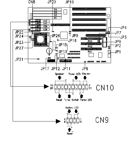
Note - The blackened pin of a jumper represents pin 1.
CPU Jumper Settings
| JP17 | JP21* | JP26 | JP27 | |
|---|---|---|---|---|
| Intel | ||||
| 25 MHz | 1-5 | 2-3 | 1-2 | 1-2 |
| 33 MHz | 2-6 | 2-3 | 1-2 | 1-2 |
| 50 MHz | 1-5 | 2-3 | 1-2 | 1-2 |
| 66 MHz | 2-6 | 2-3 | 1-2 | 1-2 |
| 100 MHz | 2-6 | 2-3 | 1-2 | 1-2 |
| AMD | ||||
| 66 MHz | 2-6 | 2-3 | 2-3 | 2-3 |
| 100 MHz | 2-6 | 2-3 | 2-3 | 2-3 |
| *NB on most systems JP21 was replaced by a solder link | ||||
Jumper Settings
| Jumper | Setting | Function |
|---|---|---|
| JP1 Password | 1-2* 2-3 | Check Password Bypass Password |
| JP2 BIOS Select | 1-2* 2-3 | Acer BIOS OEM BIOS |
| JP8 M5115 Func. | 1-2* 2-3 | Enable M5115 Disable M5115 |
| JP9,JP20* CPU Type | 1-2,2-3 2-3,1-2 | P24D/P24T (Overdrive) 486-S |
| JP11 IDE I/O address | 1-2* 2-3 | Local IDE I/O address select 0FXH Local IDE I/O address select 07XH |
| JP12 | 1-2 2-3* | Disable local IDE Enable local IDE |
| JP22 DX4 Clock | 1-2 2-3 3-4 | x 3 (tripled) x 2.5 x 2 (doubled) |
| JP23 | 1-2* 2-3 | Enable reset button Disable reset button |
| JP24 | 1-2 2-3* | Reset becomes Suspend function Normal reset function |
| Non-Configurable Jumpers | ||
| JP3 | 3-4 | |
| JP4 | 1-2, 3-4, 5-6 | |
| JP6 | 2-3 | |
| JP7 | 2-3 | |
| JP10 | 1-2 | |
Connector Functions
| Connector | Function |
|---|---|
| NC1 | Serial port 2 |
| NC2 | Serial port 1 |
| NP1 | Parallel port |
| CN1 | Game port connector |
| CN3 | Secondary IDE connector |
| CN4 | Primary IDE connector |
| CN5 | Floppy drive connector |
| CN8 | HDD LED connector |
| CN9 | Acer Multifunction connector |
| CN10 | Multifunction connector |
Memory
4/8/16 MB 72 Pin, 70ns, Non-Parity Fast Page Mode SIMMS with gold tips. You cannot mix and match parity and non-parity memory within a bank. Maximum : 64MB
Cache RAM
| Data chips | Tag chip | JP13 | JP15 | JP16 | ||
|---|---|---|---|---|---|---|
| U38-41 | U47-50 | U31 | ||||
| 128K | 32K x 8 | empty | 32K x 8 | 2-3 | 2-3 | 1-2 |
| 256K | 32K x 8 | 32K x 8 | 32K x 8 | 2-3 | 1-2 | 2-3 |
| 512K | 128K x 8 | empty | 32K x 8 | 1-2 | 1-2 | 1-2 |