Acer File Extensions |
Acer V10 Motherboard
Jumper and Connector Layout
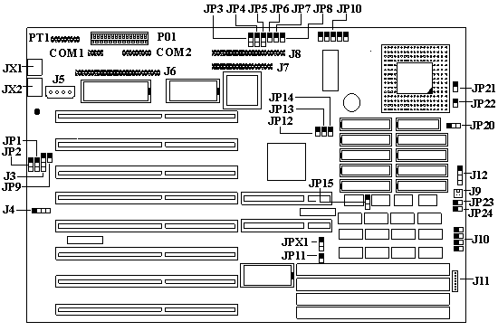
Note - The blackened pin of a jumper represents pin 1.
The Motherboard is designed on a four-layer 220x310mm printed circuit board. All system chipsets, Glue Logic Chips and other components as listed below are on the Motherboard.
- PQFP CPU -- FOR 80486SX AND 80486DX
- PGA CPU -- Intel 80486SX, 80486DX, 80486DX2
- System Control Chipset -- Acer M1419 A2
- System Data Buffer Chipset -- Acer M1421
- Video Chipset -- Cirrus Logic GD5424 OR GD5426
- VESA VL-BUS Controller -- Two 16R6Bs and One 16LB PALs
- System I/O Chipset -- Acer M5105 A4
- EPA Chipset -- Acer M6357
- Keyboard Controller -- 8042
- Real Time Clock -- DS12885
- Battery -- BR1225-IVC, 3.0V
- System ROM -- 27010-15/28F010-15
- System Cache Data -- 8K BY 8 AND 32K BY 8 20NS 28-PIN DIP SRAM
- System Cache TAG -- 8K BY 8 28-PIN AND 16K BY 4 20NS 24-PIN DIP SRAM
- Video DRAM -- 256K BY 16, 70NS IN SMD AND 256K BY 4, 70NS IN DIP
- System SIMMS -- (4 SIMM Sockets)
- 256K x 36BIT, 72 Pin 70ns, Single Sided
- 1M x 36BIT, 72 Pin 70ns, Single Sided
- 2M x 36BIT, 72 Pin 70ns, Double Sided
- 4M x 32BIT, 72 Pin 70ns, Single Sided
- Slot Connectors -- One 2R 98P ST D2.54MM
- HDD Connector -- ML 2R39P ST D2.54 L7
- FDD Connector -- ML 2R33P ST D2.54 L7
- Parallel Port: Bi-Directional or Uni-Directional
- COM1/2 -- ML 2R 9P RT HOOK GF
- Feature Connector -- ML 2R26P ST D2.54MM
- VGA Connector -- FML 3R 15P RT HOOK GF
Jumpers & Connectors
Jumpers
| Jumper | Setting | Function |
|---|---|---|
| JP1 | 1-2 | Enable Password Check |
| 2-3 | Disable Password Check | |
| JP3 | 1-2 | IRQ10 (SCSI IRQ Channel Select) |
| 2-3 | IRQ11 (SCSI IRQ Channel Select) | |
| OPEN | Disable SCSI | |
| JP4/JP5 | 1-2/1-2 | Select SCSI DMA Channel 5 |
| 2-3/2-3 | Select SCSI DMA Channel 6 | |
| OPEN/OPEN | Disable DMA | |
| JP6 | OPEN | SCSI I/O Address 340h - 35Fh |
| CLOSED | SCSI I/O Address 140h - 15Fh | |
| JP7 | OPEN | Disable On-board M5105 Function |
| CLOSED | Enable On-board M5105 Function | |
| JP8* | OPEN | Enable Parallel Port Bi-Direction Function |
| CLOSE | Enable Parallel Port Bi-Direction Function | |
| JP9 | OPEN | Use External Battery Connector |
| CLOSE | Use On-board Battery | |
| JP10 | 1-6 | 20MHZ CPU Speed |
| 2-7 | 25MHZ CPU Speed | |
| 3-8 | 33MHZ CPU Speed | |
| 4-9 | 40MHZ CPU Speed | |
| 5-10 | 50MHZ CPU Speed | |
| JP11 | OPEN | Zero Wait Write Cycle for Vesa |
| CLOSE | One Wait Write Cycle for Vesa | |
| JP15 | 1-2 | Enable On-board 4MB Dram |
| 2-3 | Disable On-board 4MB Dram | |
| JP23 | OPEN | Disable Reset Button Function |
| CLOSE | Enable Reset Button Function | |
| JP24 | OPEN | Enable Keylock Function |
| CLOSE | Disable Keylock Function |
* Note: This system uses the older 5105 chip set and therefore does not support a wide variety of applications that use a bi-directional mode. There is no work around and eaccording to Acer applications will either work or they won't.
Connectors
| Connector | Function |
|---|---|
| J1 | AT Keyboard Connector |
| JX1 | PS/2 Keyboard Connector |
| JX2 | PS/2 Mouse Connector |
| J3 | External Battery |
| J4 | VGA Control For EPA |
| J5 | HDD/FDD Power |
| J6 | SCSI Connector |
| J7 | FDD Connector |
| J8 | IDE HDD Connector |
| J9 | Fan Power |
| J10 | LED Board |
| J11 | PS/2 Keyboard/Mouse |
| J12 | HDD/LED |
| P01 | Power Connector |
| PT1 | Parallel Port Connector |
| COM1 | COM1 Port Connector |
| COM2 | COM2 Port Connector |
Memory
The system comes standard with 4MB of memory on-board and four empty 72-pin SIMM sockets. The on-board memory is the same as having 4MB of memory in Bank 0, so if the 4MBs of onboard memory is enabled DO NOT put any SIMMs in Bank 0. The board accepts 4-/16-MB Simms, recommend 72 Pin, 70ns, Parity, Fast Page Mode SIMMS with gold tips upto a maximum of 64MB . NOTE: The V10 shipped with parity SIMMs, but you can use non-parity as long as they are all non-parity.
Cache
The V10 is upgradable to 64KB, 128KB, or 256KB Cache.
| Cache Sizes | |||
|---|---|---|---|
| Cache Socket | 64KB | 128KB X 8 | 256KB X 8 |
| U59 (TAG)* | 32KB X 8 | 32KB X 8 | 32KB X 8 |
| U60,U62,U79,U81 | 8KB X 8 | 32KB X 8 | 32KB X 8 |
| U61,U63,U80,U82 | 8KB X 8 | N/A | 32KB X 8 |
*In most cases the TAG chip is soldered down. Some systems may have an empty socket.
Use ONLY 20ns Chips
| Cache Size | JP20 | JP21 | JP22 |
|---|---|---|---|
| 64KB | 2-3 | OPEN | OPEN |
| 128KB | 1-2 | CLOSE | OPEN |
| 256KB | 2-3 | CLOSE | CLOSE |