Acer File Extensions |
Acer V50LA Motherboard
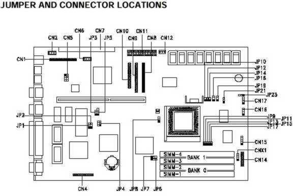
Note - The blackened pin of a jumper represents pin 1.
- CPU: Pentium 75/90/100/120/133/150/166 MHz
- Memory: Four SIMM sockets that support up to 128MB of system memory using 32-MB 70ns fast-page or EDO-type SIMMs
- Video Memory: 1-MB video memory onboard upgradable to 2-MB using 70ns video memory chips
- Cache:
- 16-KB internal cache
- 256-KB asynchronous (15ns 32K*8 SRAMs) or synchronous manufacturing optional pipeline-burst (15ns 32K*32 SRAMs) second level cache
- BIOS:
- 128-KB Flash ROM with system BIOS
- SST Flash RON 29EE010
- WINBOND Flash ROM 29EE011
- Intel Boot Block mode Flash ROM 28F001
- Video Support: Supports a maximum resolution of 1280x1024 (ATI 264CT PCI VGA accelerator onboard)
- Audio Support: Supports line-in, line-out, mic-in, and MIDI/game port (Crystal 4232 and Yamaha 289 OPL3L onboard)
- Hard Disk Interface: Two embedded PCI Enhanced IDE interfaces support up to four IDE devices
- Diskette Drive Interface: One diskette drive interface that supports 2.88/1.44/1.2-MB diskette drives. Supports three-mode diskette types.
- Onboard I/O: One PS/2 Keyboard and one mouse port. Two NS16C550-compatible serial ports and one parallel port that supports EPP/ECP modes
- Real-time Clock: System clock/calendar with 128 bytes CMOS RAM
- Expansion Slots:
- Desktop Models:
- One ISA slot
- Two PCI/ISA slots
- Minitower Models:
- Four ISA slots, One ISA/PCI slot
- Three PCI slots
- Desktop Models:
- Power Supply: 145-watt 115v/230v switching power supply
Jumper Settings
| Jumper | Setting | Function | |||||||||||||||
|---|---|---|---|---|---|---|---|---|---|---|---|---|---|---|---|---|---|
| JP1 BIOS Type | 1-2 2-3* | For models with Acer BIOS For models with OEM BIOS | |||||||||||||||
| JP2 Password Check | 1-2 2-3* | Check password Bypass password | |||||||||||||||
| JP3 Boot Block Feature ** | 1-2 2-3* | Enable Flash ROM boot block feature Disable Flash ROM boot block Feature | |||||||||||||||
| JP5 BIOS ROM Type | 1-2 2-3 3-4* | EPROM Flash ROM (Intel 28F010, 28F001) Flash ROM (SST, Winbond 29EE010) | |||||||||||||||
| JP4 CPU Core/Host Bus Frequency | 1-4 2-5* 3-6 | 75/50 MHz 90/60, 120/60, 150/60 MHz 100/66, 133/66, 167/66 MHz | |||||||||||||||
| JP6,JP7 Second-level Cache | 1-2*,1-2* | 256 KB All other settings reserved | |||||||||||||||
| JP8 CPU Type | 1-2* 2-3 | Intel P54C or AMD K5 Cyrix M1 | |||||||||||||||
| JP16,JP19 CPU / Clock Ratio |
|
| |||||||||||||||
| JP21 CPU Voltage | 1-2* 2-3 | 3.38V for VR and standard CPU type 3.52V for VRE CPU type | |||||||||||||||
| JP23 LED Support | 1-2 2-3* | For IDE and diskette drives For IDE drive only |
| ** The boot block feature works only with Intel 28F001 Flash ROM and requires JP5 to be set to pins 2-3. *Default setting. |
Connector Functions
| Connector | Function |
|---|---|
| CN1 | Audio/MIDI connector |
| CN2 | Fax/voice modem connector |
| CN4 | Video feature connector |
| CN5 | WaveTable connector |
| CN6 | CD-audio line-in connector |
| CN7 | Feature connector for nultimedia or Ethernet solution |
| CN8 | IDE channel 1 |
| CN9 | IDE channel 2 |
| CN10 | Diskette drive connector |
| CN11 | Power connector |
| CN12 | Standby power connector |
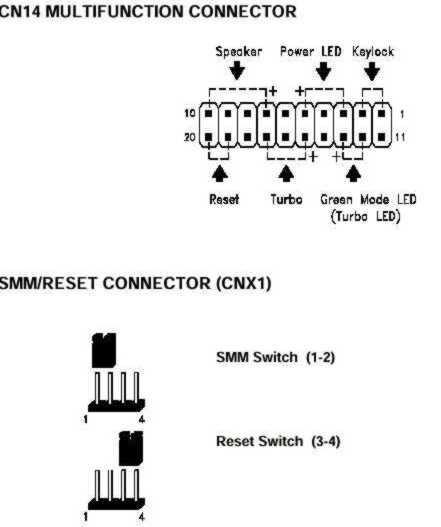
| CN14 | Multifunction connector |
| CN15 | IrDA connector |
| CN16 | Hard disk drive LED connector |
| CN17 | Hard disk drive LED connector (generic) |
| CNX1 | SMM switch/Reset switch |