Acer File Extensions |
Packard Bell 540/550/560 M/Board
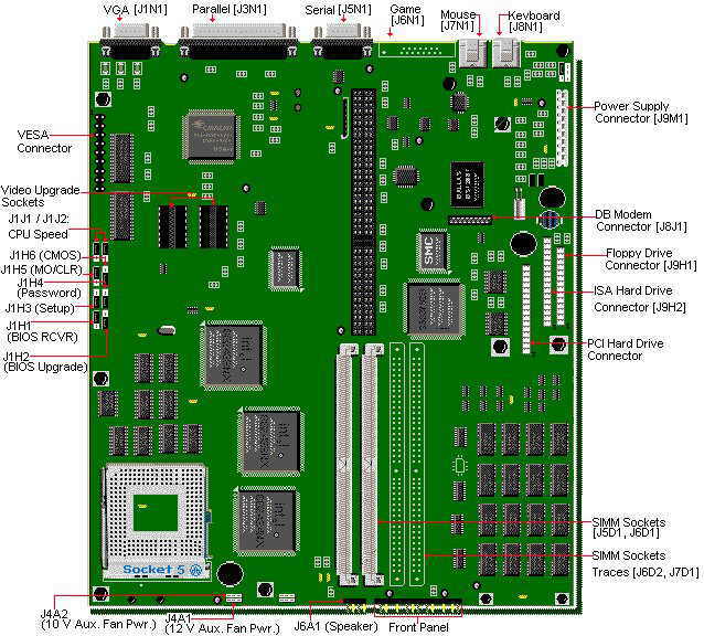
Installing a video expansion card will automatically disable the onboard video controller.
Specification
- Battery : Integrated into the Real Time Clock (RTC)- DallasÛ DS12887 chip. The internal battery in the DS12887 device has an estimated lifetime of ten years.
- BIOS : Flash EEPROM - AMI BIOS.
- Bus Architecture : PCI 2.0/ISA based system bus Intel Neptune PCI Chipset.
- Cache : 16K level 1 cache 256k level 2 cache.
- Chipset :
- S82434NX PCI/Cache/Memory Controller.
- FDC37C665GT Super I/O Controller.
- S82378ZB System Controller.
- S82433NX Local Bus Extension.
- RZ1000BP PCI IDE Processor.
- CPU :
- Pentium 75 MHz (PB540).
- Pentium 90 MHz (PB550).
- Pentium 100 MHz (PB560).
- Uses 320 pin Type 5 CPU Zero Insertion Force (ZIF) CPU Socket.
- Interfaces :
- 1 DB-9 Serial ports for COM1.
- 1 DB-25 Parallel port.
- 1 PS/2 Keyboard port.
- 1 PS/2 Mouse port.
- 1 15 pin VGA.
- RAM : 8MB standard 72/136MB maximum Uses 4/8/16/32MB 72-pin SIMMs, @ 70ns.
- Speaker : External 8 Ohms, 1/2 Watt speaker.
- UART : 16C550A Compatible.
- Video : Built-in, Cirrus LogicÛ Alpine GD5434.
- Video RAM : Upgradable to 2 MB.
Jumpers
| Jumper | Function | Pin/Setting | Description |
|---|---|---|---|
| J1H1 | Flash Boot Block | 1-2 2-3 | Recovery Mode Normal Mode * |
| J1H2 | Flash Write | 1-2 2-3 | Enabled * Protected |
| J1H3 | CMOS Setup | 1-2 2-3 | Enable * Disable |
| J1H4 | Password | 1-2 2-3 | Normal * Clear |
| J1H5 | VGA Mode | 1-2 2-3 | Monochrome Colour * |
| J1H6 | CMOS Clear | 1-2 2-3 | Normal * Clear |
| J1J1 | CPU Speed | 1-2 2-3 | 75MHz 90MHz |
| J1J2 | Clock Multiplier | 1-2 2-3 | x1.5 x1.0 |
| J9N1 | CPU Voltage Sel. | 1-2 2-3 | 3.45V 3.3V |
* Indicates default value.
Battery
The battery is a Dallas DS 12887 real time clock and CMOS battery integrated into the RTC chip.
BIOS
The BIOS in the PB540/550/560 is contained in Flash EEPROM, and it can be updated via software. If the Flash BIOS is corrupted during an update, it is possible to recover it.
To run the BIOS update,
1. Insert the update diskette into drive A: and reboot the system.
2. When the opening dialogue appears, press (enter).
3. The Main Menu will appear on the screen.
4. Select "Update Flash Memory Area from a file" using the Down Arrow key.
5. Press (enter).
6. The UPDATE FLASH AREA dialog box appears on the screen.
7. Select "Update System Bios".
8. Press (enter).
9. Press the Down Arrow key to select 1007BC0R.BIO file.
10. Press (enter).
11. Highlight the (continue with programming)option and press (enter).
12. Remove the disk from drive A and press (enter).
BIOS Recovery
To recover from a corrupted BIOS, perform the following steps:
1. Turn off the system.
2. Remove the system's case and move the jumper block on J1H1 from pins 2-3 to pins 1-2. Leave the jumper block on J1H2 pins 1-2 in place.
3. Place the update diskette in drive A: and turn on the system.
4. There will be no video display during the BIOS recovery, this is due to the small amount of code available in the non-erasable boot block area.
5. After the system boots, it will beep once and the floppy drive light should light up. The system is copying the recovery code into the Flash EEPROM.
6. Just before the recovery completes, the system will beep twice. Once this occurs, watch the floppy drive light. When the light goes off, turn off the system.
7. Move the jumper block on J1H1 from pins 1-2 back to pins 2-3.
8. Turn the system on and repeat the steps for updating the BIOS.
Cache Upgrade
Comes with 16KB internal cache (integrated into the CPU), and 256KB Secondary External Cache (Soldered on-board).This is not upgradable.
CPU Upgrades
Each motherboard can accommodate the following CPUs:
- Intel Pentium 75MHz
- Intel Pentium 90MHz
- Intel Pentium 100MHz
The PB540/550/560 is only upgradable with the Pentium Overdrive for Pentium Systems.
| CPU Type | J1J1: CPU Base Speed | J1J2: Clock Multiplier |
|---|---|---|
| Pentium 75MHz | 1-2 | 2-3 |
| Pentium 90MHz | 2-3 | 2-3 |
| Pentium 100MHz | 1-2 | 1-2 |
Memory Upgrades
SIMM speed must be 70ns or faster.
The SIMMs are 4/8/16/32MB 72-pin and can be x32 or x36. The motherboard design does not require parity checking, hence x32 simms can be purchased.The motherboard will not use EDO, only Fast Page Mode SIMMs will operate correctly in this motherboard.
Some motherboards may have 2 or 4 SIMM sockets. Therefore, allowing a maximum of either 72 or 136 MB.
SIMMs are inserted in Bank A or B, sockets J5D1 - J6D1. One Bank must be filled when the upgrade is done. Some systems may have a second bank (A) for a maximum of 136MB.
Video Memory Upgrade
The PB540 can be upgraded to 2MB video memory using two 256Kx16-70ns SOJ DRAM chips.The video memory upgrade is inserted in sockets U10A1 and U11A1. Pin 1 is at the front right corner of the socket. To install the chip, insert it into the socket and push it on the chip until it snaps into place.