Acer File Extensions |
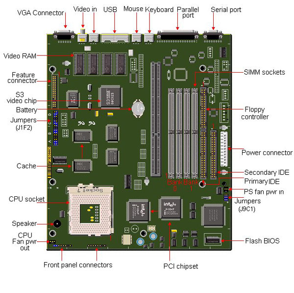
Packard Bell 685 M/Board
. If a new video card is installed, the new video card's display `overrides' the display of the onboard video. Device Manager, however, will continue to list the onboard video as a display adapter.
Specification
- Battery : Socketed 3 volt Lithium coin cell battery at location BT5G1.
- BIOS : Flash EEPROM - AMI BIOS.Plug and Play 1.0a spec, support for Windows 95.
- Bus Architecture : PCI 2.1/ISA based system bus.66MHz maximum bus speed
- Cache : 16K level 1 cache.May have 256KB Pipelined Burst Cache soldered on board, not upgradable.
- Chipset : Intel Triton II 82430VX PCI set.
- CPU :
- Pentium 75 MHz
- Pentium 90 MHz
- Pentium 100 MHz
- Pentium 120 MHz
- Pentium 133 MHz
- Pentium 150 MHz
- Pentium 166 MHz
- Intel MMX Pentium 166 MHz
- Intel Pentium 200 MHz
- Intel MMX Pentium 200 MHz
- Uses Type 7 Zero Insertion Force (ZIF) CPU Socket.
- Supports Pentium Overdrive.
- Form Factor : LPX
- Interfaces :
- Serial DB-9 Serial port for COM1
- Parallel DB-25 Parallel port
- Keyboard PS/2 keyboard port
- Mouse PS/2 mouse port
- S-Video I2C and S-video IN
- USB Side-by side USB connector
- VGA DB-15 VGA port
- FDD Connector 34-pin on-board header connector
- HDD Connector 40-pin PCI IDE (fast PIO-4)
- HDD Connector 40-pin PCI IDE (fast PIO-4)
- VESA Feature Connector 34-pin header connector
- PCI Chipset : Intel Triton 82430VX PCI chipset
- RAM : 8MB installed standard/128MB maximum.Uses 4/8/16/32 MB 72-pin SIMMs, 60 or 70ns, EDO or Fast Page RAM Supports only non-parity DRAM.
- Riser Card : Desktop Case - 2xISA, 1xPCI, 1xPCI/ISA.Minitower Case - 2xISA, 2xPCI, 1xPCI/ISA.
- Speaker : On-board piezo speaker.
- UART : Two 16C550A Compatible chips.
- Video : Built-in, S3 Trio64V+ or S3 Virge 3D PCI graphics controller:
- 1024 x 768, 256 colours with 1MB
- 1280 x 1024, 256 colours with 2MB
- VESA Display Channel supported.
- DPMS compliant.
- Video RAM : S3 Trio64V+ motherboards have 1MB expandable to 2MB.S3 Virge 3D motherboards have 2MB Non Upgradable.
Jumpers
| Function | Location | Jumpers | Configuration |
|---|---|---|---|
| Host Bus Speed * | J1F2C | 1-2, 5-6 2-3, 4-5 2-3, 5-6 | 66MHz 60MHz 50MHz |
| CPU Clock Ratio | J1F2D | 1-2, 4-5 2-3, 4-5 2-3, 5-6 1-2, 5-6 | x1.5 x2.0 x2.5 x3.0 |
| CMOS Clear | J1F2A | 4-5 5-6 | Normal Clear |
| Password Clear | J1F2A | 1-2 2-3 | Password Enabled Password Disabled |
| CMOS Setup Access | J1F2B | 1-2 2-3 | Enabled Access Denied |
| Processor Voltage | J1F2B | 4-5 5-6 | Standard Voltage (3.3v) VRE |
| Recovery Mode | J9C1 | 1-2 2-3 4-5, 5-6 | Normal Recovery Reserved |
* Note: PCI clock speed equals � Host bus speed
Battery
This 3V Lithium clip in battery is replaceable with a CR2032 battery.
Flash Bios Update
Bios Upgrade Procedure
- Insert the BIOS update diskette into drive A: and reboot the system.
- Press Enter when the first screen appears.
- Select "Update Flash Memory Area from a file" using the Down Arrow key.
- Press Enter.
- The UPDATE FLASH AREA dialog box appears on the screen.
- Select "Update System Bios" and press Enter.
- Select 1006DN0R.BIO file and press Enter.
- Press Enter at the following screen to proceed with programming.
- The BIOS is now re-programmed with the updated BIOS file.
- Remove the disk from drive A.
- Press Enter to reboot the computer system.
- Complete the process by running the CMOS Setup program.
Bios Upgrade Procedure
- The 'FLASH NORMAL/FLASH RECOVERY' jumper block,J9C1 is located near the Primary Power Connector,J9E2.
- Move the 'FLASH NORMAL/FLASH RECOVERY' jumper block,J9C1 from pins 1-2, 4-5 to pins 2-3, 5-6.
- Insert the BIOS upgrade diskette and reboot the system. No video is available during the procedure.
- The system beeps once and starts copying the recovery code into the CMOS Flash memory. The system beeps twice as the recovery completes.
- Turn off the system and move the jumper block,J9C1 from pins 2-3, 5-6 to pins 1-2, 4-5.
- Leave the BIOS upgrade diskette in the floppy drive, and continue with the original upgrade following the procedure described in 'BIOS UPGRADE PROCEDURE'.
Cache Upgrade
The motherboard comes with:
16KB L1 (Internal) write-back cache (integrated in the CPU)
256KB L2 (External) write-through with write buffers cache soldered on the motherboard.Not upgradeable.
Note :Some motherboards may come with no L2 cache and are also not upgradeable.
CPU Upgrades
This motherboard can accommodate the following CPUs:
- Intel Pentium 75 MHz
- Intel Pentium 90 MHz
- Intel Pentium 100 MHz
- Intel Pentium 120 MHz
- Intel Pentium 133 MHz
- Intel Pentium 150 MHz
- Intel Pentium 166 MHz
- Intel Pentium 200 MHz
| Clock Speed (J1F2C) | CPU Multiplier (J1F2D) | Host Bus Speed | CPU Speed |
|---|---|---|---|
| 2-3, 5-6 | 1-2, 4-5 (x 1.5) | 50 MHz | 75 MHz |
| 2-3, 4-5 | 1-2, 4-5(x 1.5) | 60 MHz | 90 MHz |
| 1-2, 5-6 | 1-2, 4-5(x 1.5) | 66 MHz | 100 MHz |
| 2-3, 4-5 | 2-3, 4-5(x 2.0) | 60 MHz | 120 MHz |
| 1-2, 5-6 | 2-3, 4-5(x 2.0) | 66 MHz | 133 MHz |
| 2-3, 4-5 | 2-3, 5-6(x 2.5) | 60 MHz | 150 MHz |
| 1-2, 5-6 | 2-3, 5-6(x 2.5) | 66 MHz | 166 MHz |
| 1-2, 5-6 | 2-3, 5-6(x 2.5) | 66 MHz | 166 MMX |
| 1-2, 5-6 | 1-2, 5-6(x 3.0) | 66 MHz | 200 MHz |
| 1-2, 5-6 | 1-2, 5-6(x 3.0) | 66 MHz | 200 MMX |
On later PB685 motherboards an enginering revision was made that removed pins 1 and 2 from jumper J1F2D.Below are the correct settings for CPU multiplier speeds.Other jumper settings remain the same.
| CPU Multiplier | 2-3 | 5-6 |
|---|---|---|
| 1.5x | out | out |
| 2.0x | in | out |
| 2.5x | in | out |
| 3.0x | out | in |
| 3.5x | out | out |
Uses the 321-pin Type 7 Zero Insertion Force (ZIF) CPU socket.
Supports the Pentium OverDrive Processor.
Not keyboard switchable.
Disable cache to slow down the system.
RAM Upgrades
Uses 4/8/16/32 MB 72-pin simms, 60 or 70ns EDO (See below) or Fast Paged RAM up to a maximum of 128MB.Supports only non-parity DRAM.
1. Bank by bank support for EDO or Fast Page Mode DRAM with automatic presence detect for EDO DRAM. 60ns EDO required for 66 MHz bus speeds, and 70ns EDO required for 50 & 60 MHz bus speed. 70ns Fast Page Mode required for 50, 60, and 66 MHz bus speeds. EDO and Fast Page Mode can be mixed in separate banks.
2. Four 32 bit SIMM sockets 4 MB, 8 MB, 16 MB, 32 MB in either single or double sided configurations. Simms mustbe added in pairs. SIMM sockets can be populated in any order. ONE or more simms may be located under the peripheral bay in the Packard Bell "all-in-one" (Spectria) chassis.
3. Bank 0 will be populated as the default from the factory.
4. No configuration jumpers: BIOS detects memory size, and memory type (EDO or Fast Page Mode).
5. Memory voltage requirements: 5V.
Video Memory Upgrade
The PB680 uses S3 Inc. Trio64V+ or S3 Virge 3D PCI Video Chipset.
S3 Trio64V+ motherboards have 1MB expandable to 2MB using two 256Kx16-50ns SOJ EDO DRAM chips.
S3 Virge 3D motherboards have 2MB Non Upgradable.
The video memory upgrade is inserted in sockets U2J1 and U3J1. Pin 1 is at the front right corner of the socket. To install the chip, insert it into the socket and push until the chip snaps into place.